Laser Diode & Array Driving
A laser diode is a current-driven device, not a voltage-driven one. Its optical output tracks the current through the junction, and the junction tolerates very little of the transient current a poorly regulated supply can produce. Above turn-on the current rises steeply with forward voltage (Figure 1), so a diode driven from a stiff voltage source turns a small change in forward voltage into a large, uncontrolled swing in current, which appears as an unstable optical pulse or, at worst, a damaged emitter. The job of a diode driver is to deliver a defined current with a defined edge, hold it flat for the pulse, and return cleanly to zero, while keeping the device safe through power-up, power-down, and fault conditions.
Berkeley Nucleonics, through its Directed Energy Division, builds current-source drivers for this work. The lineup runs from a 3 A precision source for a single emitter to the 450 A PCX-7500-EX for large bars and stacked arrays, with one support path across the range.
The challenge
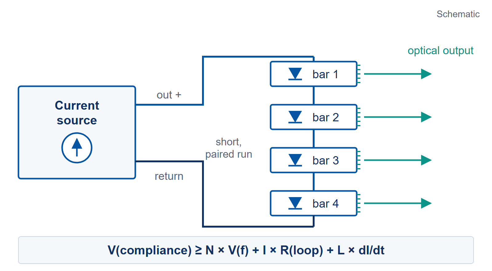
Three problems sit at the center of diode and array driving. The first is current control. The pulse the emitter sees has to match the pulse the experiment asked for, in amplitude, in width, and in edge speed, without overshoot that pushes the junction past its rated current. The second is compliance voltage. A current source can only force its programmed current if it has enough voltage headroom to overcome the forward drop of the diode string plus the resistive and inductive drops in the cabling. Stack more bars in series and the required compliance climbs, so the driver has to carry margin or the pulse flattens and distorts.
The third problem is protection. A diode array represents a large investment, and a single fault can take it out in microseconds. The driver has to guard against reverse voltage, has to limit current under a short, and has to leave the output in a safe state whenever it is disabled rather than floating in a way that could stress the load. Cabling matters here too. Series inductance in the path between driver and diode slows the edge and rings the pulse, so the physical connection is part of the circuit, not an afterthought.
The BNC approach
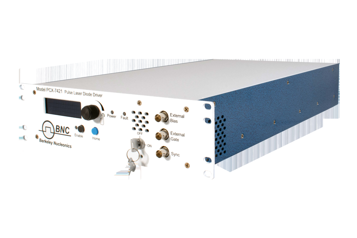
DEI drivers are current sources with the output stage and protection treated as one system (Figure 2 shows the PCX-7421). The user programs current, and the driver holds that current across the pulse as long as the load stays inside its compliance window, which each datasheet states so a system designer can budget headroom against the diode string before ordering. This matters most in QCW operation, where the device runs quasi-continuous-wave bursts that sit between short pulsed shots and full CW drive. QCW lets an array reach high peak optical power without the continuous thermal load of true CW, and it depends on a driver that holds a long, flat current pulse rather than a short spike.
Output protection is part of the design. The PCX-7401 and PCX-7421 short the output to ground at turn-on and whenever the output is not enabled, so no current flows through the diode while the instrument is idle, and both gate the output with a key switch and an interlock. The PCO-6131 and PCO-6141 modules disable the output if the +24 VDC supply falls below 18 V, include clamp diodes that protect the diode against reverse voltage, and store about 7 J in the regulator, which limits the energy available to the diode in a fault. The PCX-7500-EX output connector is interlocked, so the source is disabled when the connector is removed. To keep the delivered edge clean, use low-inductance cabling kept as short and as tightly paired as the layout allows: the PCX-7401 and PCX-7500-EX are specified with a stripline interconnect of less than 4 nH, the PCX-7421 with low-inductance twisted pair, and the PIM-Mini-200 with 10 cm of 22 AWG twisted pair.
A worked compliance budget shows how the choice narrows. Assume four bars in series at 2.0 V each: they drop 8.0 V, and at 100 A, 5 mΩ of cable and connector resistance adds 0.5 V, for 8.5 V before the inductive term on the edge. That string fits the 20 V forward-voltage limit of the PCO-6131 with margin. On the PIM-Mini-200 the DC input is set 12 V above the forward voltage, here about 20.5 V, inside its 12 V to 60 V range. Longer strings move to the PIM-Mini-200 (forward voltage to 48 V) or the PCX-7500-EX, whose external supply provides up to 110 V. The PIM-Mini-200 and PCX-7500-EX are microsecond-class sources built for long QCW pulses, while the PCX-7421 and the PCO modules provide nanosecond-class edges.
Recommended instruments
Match the driver to the load. Start from the diode string: count the series voltage drop, add cabling drops, and pick a driver whose compliance carries margin above that total at your target current.
- PCX-7401: 0 to 3 A pulsed plus a 0 to 0.550 A bias output, both in 1 mA steps; 15 V compliance; rise and fall 100 ns or less; pulse width 100 ns to DC; internal trigger 5 Hz to 1 MHz. For single emitters and L-I characterization.
- PCX-7421: 50 mA to 21.5 A pulsed or QCW, 3.0 A to 5.8 A CW, bias to 5.8 A; 24 V compliance; rise under 25 ns; pulse width 50 ns to 500 ms. For bars and small arrays that need CW and QCW modes.
- PCO-6141: OEM module, up to 60 A; rise adjustable from under 12 ns to over 1.5 µs; pulse width 100 ns (at 6 V compliance) and 200 ns to DC; single shot to 500 kHz; diode forward voltage to 20 V.
- PCO-6131: OEM module, up to 125 A; rise adjustable from under 30 ns to over 2.5 µs; pulse width under 100 ns to DC; single shot to 500 kHz; diode forward voltage to 20 V.
- PIM-Mini-200: 25 A to 200 A in a 0.5 kg module; pulse width 25 µs to 250 µs at up to 200 Hz; diode forward voltage 0 V to 48 V, with the DC input set 12 V above it. Rise and fall are 10 µs or less above 140 A (measured 5.82 µs rise and 3.50 µs fall at 200 A), so its edges are microsecond class.
- PCX-7500-EX: 10 A to 450 A; pulse width 4 µs to 5,000 µs at 8 Hz to 10 kHz; compliance up to 110 V from an external DC supply matched to the diode string; up to 1000 W output power; rise and fall 7 µs or less (measured 2.564 µs rise at 450 A into a 73 V load). For large bars and stacked arrays.
Getting started
Define the load first: peak current, pulse width, repetition rate, and whether the work is single-shot, pulsed, QCW, or CW. Sum the forward voltage of the series string and add headroom for cabling so you can size compliance correctly. Plan the physical connection for low inductance, keeping the run short and the conductors tightly paired, then confirm the protection behavior you need on disable and under fault. Talk to a BNC applications engineer at info@berkeleynucleonics.com or 800-234-7858, and an engineer will help match a driver to your array.