 Powered by Bioz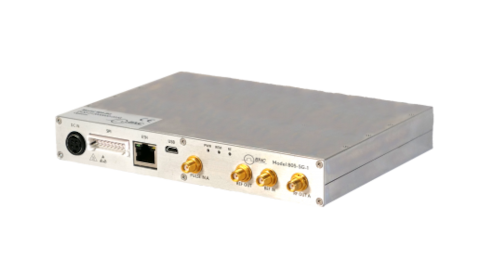
1Overview
The Model 805-SG microwave signal source modules deliver instrument-grade performance, increased functionality, and efficient power consumption at a reduced size and affordable cost. The design combines low phase noise with fast switching capability, covering a wide frequency range from 8 kHz up to 20 GHz. The low spurious and harmonic content of the signal makes it ideally suitable for many demanding applications.
The unit contains a high stability OCXO, providing accurate, power-calibrated, phase-lockable output signals. The frequency resolution is 1 mHz and the power resolution is 0.01 dB power. The unit is remotely controlled with USB, LAN or SPI control.
Due to the form-factor, the unit can also be used as a drop-in replacement of the obsolete "QuickSyn Synthesizers" from NI.
2Key Features
- Microsecond switching-speed. Fast frequency switching for agile test sequences.
- Low-phase noise and spur levels. Clean spectral output across the band.
- Portable battery option. Field-ready in a compact form.
- Low level error accuracy. Power-calibrated output.
- Compact module. 7 x 5.4 x 1 in including connectors, under 2.4 lb.
- High-stability OCXO with accurate, phase-lockable output signals.
3Signal Specifications
| Parameter | Min | Typical | Max | Note |
|---|---|---|---|---|
| Frequency range | 10 MHz 8 kHz | 20 GHz 20 GHz | settable to 22 GHz Option 8K | |
| Frequency resolution | 0.001 Hz 0.001 Hz | GUI SW setting resolution SPI interface setting resolution | ||
| Frequency switching time | 500 µs 15 µs | 20 µs | Option FS | |
| Phase adjustment range | 0 deg | 360 deg | ||
| Phase resolution | 0.1 deg |
4Phase Noise
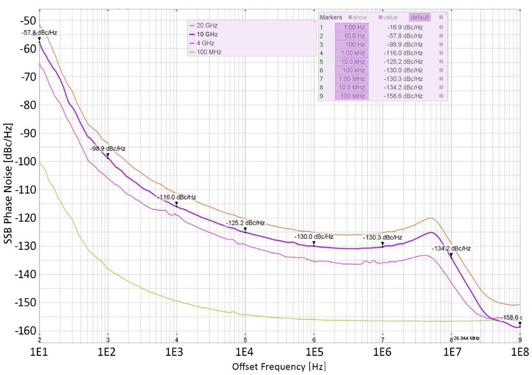
SSB phase noise (dBc/Hz), typical and maximum, by carrier frequency and offset from carrier.
| Frequency | 10 Hz Typ. | Max. | 100 Hz Typ. | Max. | 1 kHz Typ. | Max. | 20 kHz Typ. | Max. | 100 kHz Typ. | Max. | 1 MHz Typ. | Max. | 10 MHz Typ. | Max. |
|---|---|---|---|---|---|---|---|---|---|---|---|---|---|---|
| 100 MHz | -108 | -103 | -136 | -131 | -150 | -145 | -155 | -150 | -155 | -150 | -155 | -150 | -154 | -149 |
| 1 GHz | -80 | -75 | -116 | -111 | -137 | -132 | -147 | -142 | -147 | -142 | -145 | -140 | -156 | -151 |
| 2 GHz | -74 | -69 | -112 | -107 | -133 | -128 | -144 | -139 | -144 | -139 | -141 | -136 | -155 | -150 |
| 5 GHz | -65 | -60 | -101 | -96 | -126 | -121 | -136 | -131 | -138 | -133 | -136 | -131 | -148 | -143 |
| 10 GHz | -60 | -55 | -96 | -91 | -120 | -115 | -130 | -125 | -131 | -126 | -12p(verify) | -124 | -142 | -137 |
| 20 GHz | -52 | -47 | -91 | -86 | -114 | -109 | -125 | -120 | -126 | -121 | -124 | -119 | -137 | -132 |
5Spectral Purity
| Parameter | Min | Typical | Max | Note |
|---|---|---|---|---|
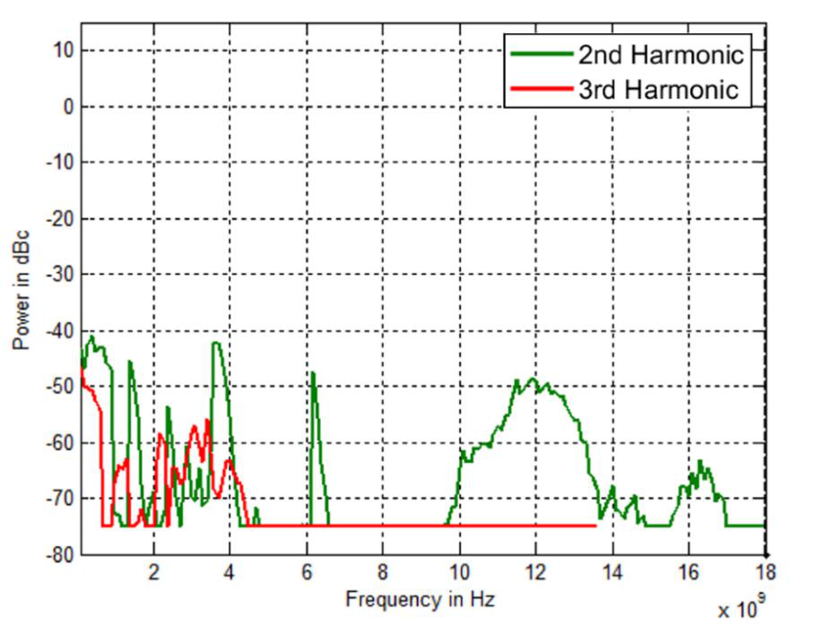
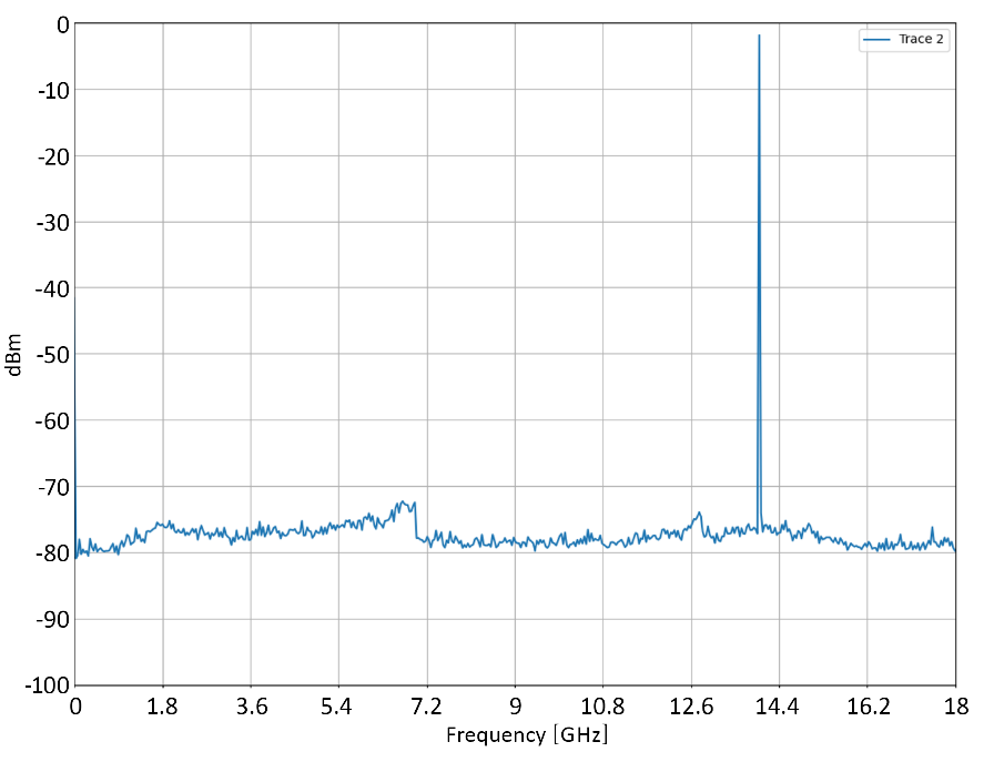
| Harmonics | At 10 dBm; See plot below | |||
| < 100 MHz | -35 dBc | |||
| 100 MHz to 20 GHz | -50 dBc | -40 dBc | ||
| 4.5 GHz to 20 GHz | -50 dBc | -40 dBc | ||
| Sub-harmonics | At 10 dBm; See plot below | |||
| < 5 GHz | -75 dBc | -65 dBc | ||
| 5 GHz to 11.5 GHz | -65 dBc | -55 dBc | ||
| 11.5 GHz to 20 GHz | -75 dBc | -65 dBc | ||
| Non-harmonic spurious | 10 kHz to 0.5 GHz offset from carrier | |||
| < 1 GHz | -65 dBc | -55 dBc | ||
| 1 GHz to 20 GHz | -70 dBc | -60 dBc |
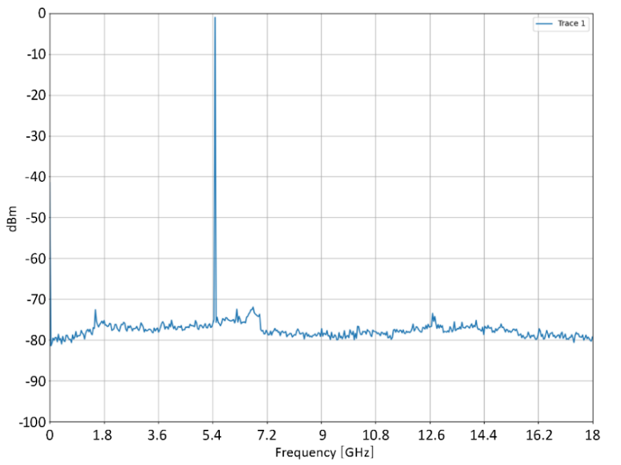
Wideband spectra confirm the low harmonic and spurious content across the operating band.
6Level Performance
| Parameter | Min | Typical | Max | Note |
|---|---|---|---|---|
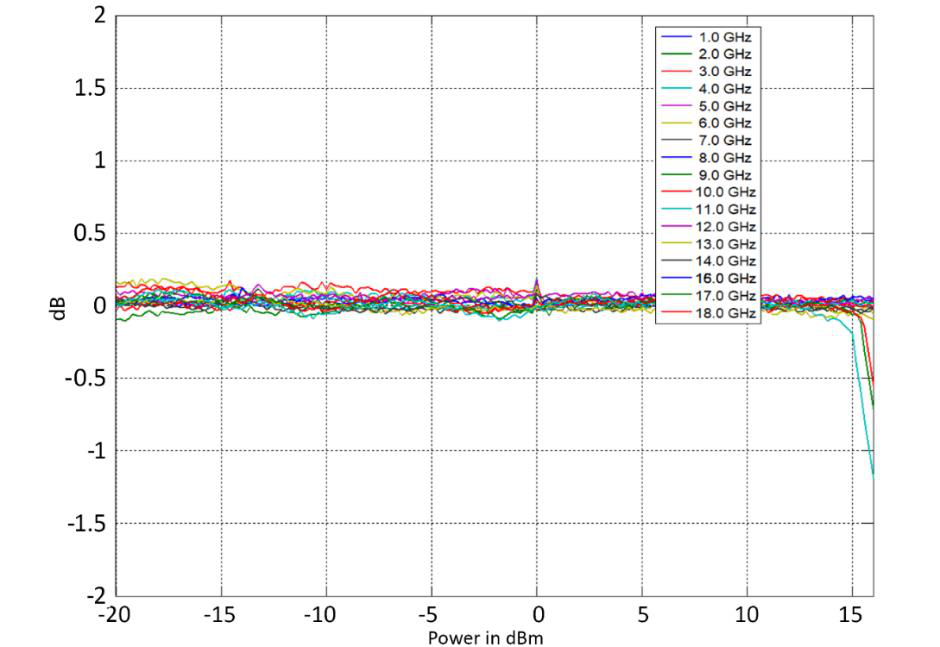
| Output power level | Settable to +25 dBm; See plot below | |||
| 8 kHz to 10 MHz | -20 dBm | 9 dBm | ||
| 10 GHz to 20 GHz | -20 dBm | 15 dBm | ||
| Power level uncertainty | 0.25 dB | 1.0 dB | -20 to 15 dBm. See plots below | |
| Power resolution | 0.01 dB | 0.1 dB | GUI SW setting resolution SPI interface setting resolution | |
| Power settling time | 1 ms 5 µs | ALC off (open loop) ALC on (closed loop) | ||
| Output impedance | 50 Ω | |||
| VSWR | 1.7 | |||
| Reverse power protection | ||||
| DC voltage | 7 V | |||
| RF power | 23 dBm |
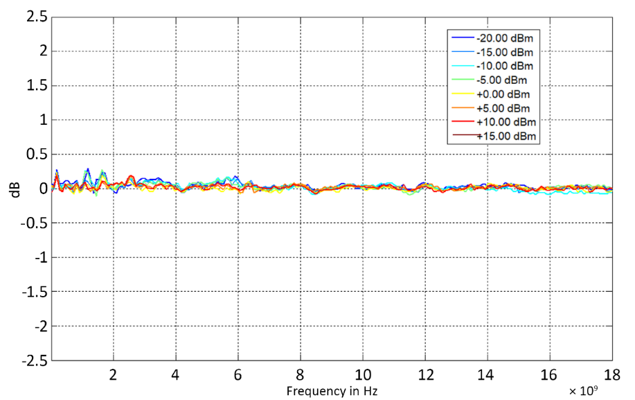
Power level linearity and frequency response remain within the stated uncertainty across the band.
7Reference Frequency
| Parameter | Min | Typical | Max | Note |
|---|---|---|---|---|
| Internal reference frequency | 100 MHz | |||
| Calibrated accuracy of int. reference | ±30 ppb | Calibrated at 23 ± 3 °C | ||
| Temperature stability (0 to 50 °C) | ±100 ppb | |||
| Aging 1st year | 500 ppb | |||
| Aging per day | 5 ppb | After 30 days operation | ||
| Warm-up time | 5 min | |||
| Reference frequency input | 10 MHz, 100 MHz, 1 GHz 10 – 250 MHz | Fixed reference frequency Variable reference frequency | ||
| Reference input level 10 MHz 100 MHz 1 GHz 10 – 250 MHz | -3 dBm -3 dBm -3 dBm -3 dBm | +12 dBm +12 dBm +12 dBm +12 dBm | Fixed reference frequency Fixed reference frequency Fixed reference frequency Variable reference frequency | |
| Variable reference frequency resolution | 100 kHz | |||
| Lock range 10 MHz 100 MHz 1 GHz 10 – 250 MHz | ±1.5 ppm ±100 ppm ±100 ppm ±1.5 ppm | Fixed reference frequency Fixed reference frequency, bypass Fixed reference frequency, bypass Variable reference frequency | ||
| Reference input impedance | 50 Ω | |||
| Reference frequency output | 10 MHz, 100 MHz, 1 GHz | Settable | ||
| Output power 10 MHz 100 MHz 1 GHz | +3 dBm +3 dBm +3 dBm | +5 dBm +5 dBm +5 dBm | +7 dBm +7 dBm +7 dBm | |
| Reference output impedance | 50 Ω |
Reference architecture. External variable reference frequencies and 10 MHz external fixed reference frequency will be internally locked to the internal 100 MHz reference with a PLL circuit. 100 MHz and 1 GHz external fixed reference frequencies are bypassing the internal reference PLL circuit and are acting directly as reference signal for the synthesizer.
8Modulation Capability
| Parameter | Min | Typical | Max | Note |
|---|---|---|---|---|
| Pulse Modulation | Option PULSE | |||
| Modulation source | Internal External (PULSE) | |||
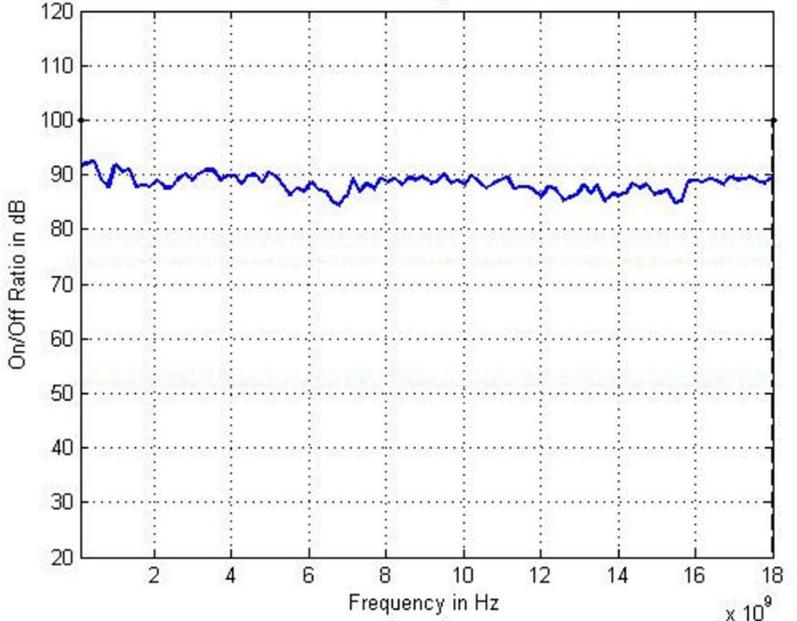
| On/off ratio < 1 GHz 1 GHz to 20 GHz | 70 dB 80 dB | 85 dB 100 dB | At 10 dBm; see plot below. | |
| Repetition frequency | 0 Hz | 10 MHz | ||
| Pulse width | 30 ns | 20 s | ||
| Pulse width compression | 20 ns | |||
| Pulse resolution | 10 ns | |||
| Pulse rise/fall time | 9 ns | 12 ns | ||
| Pulse polarity | Normal Inverse | Settable | ||
| Pulse train length | 1 | 4096 | ||
| Pulse overshoot | 10% | |||
| External pulse latency | 45 ns | 60 ns |
9Sweeping Capability
| Parameter | Min | Typical | Max | Note |
|---|---|---|---|---|
| Sweep parameters | Frequency, power, list | |||
| Number of list points | 1 | 50,000 | ||
| Sweep type | Linear, logarithmic, random | |||
| Step time | 500 µs 20 µs | 20 s 20 s | Option FS | |
| Timing resolution | 10 ns | |||
| Timing accuracy per point | 20 ns | |||
| Generalized list sweep | Allows for individual setting of frequency, step-time, and off-time for each point | |||
10Trigger (PULSE)
| Parameter | Min | Typical | Max | Note |
|---|---|---|---|---|
| Trigger types | Continuous Single (point) Gated | Gated direction | ||
| Trigger source | External (PULSE, SPI Trigger) Bus (Ethernet, USB, SPI) | |||
| Trigger modes | Continuous free run Trigger and run Reset and run | |||
| External trigger latency | 140 ns | |||
| External trigger uncertainty | 20 ns | |||
| External trigger delay | 0 s | 20 s | Settable | |
| External delay resolution | 10 ns | |||
| Trigger modulo | 1 | 255 | Execute only on Nth trigger event | |
| Trigger polarity | Rising Falling | |||
| External PULSE input threshold | 0.85 V | 0.9 V | 0.95 V | TTL compatible |
| External PULSE input voltage range | -0.5 V | +5.5 V | TTL compatible, 100 kΩ pull-up to +5.0 V | |
| External PULSE input hysteresis | 30 mV |
11Mechanical Specifications
Dimensions & Weight
| Parameter | Value |
|---|---|
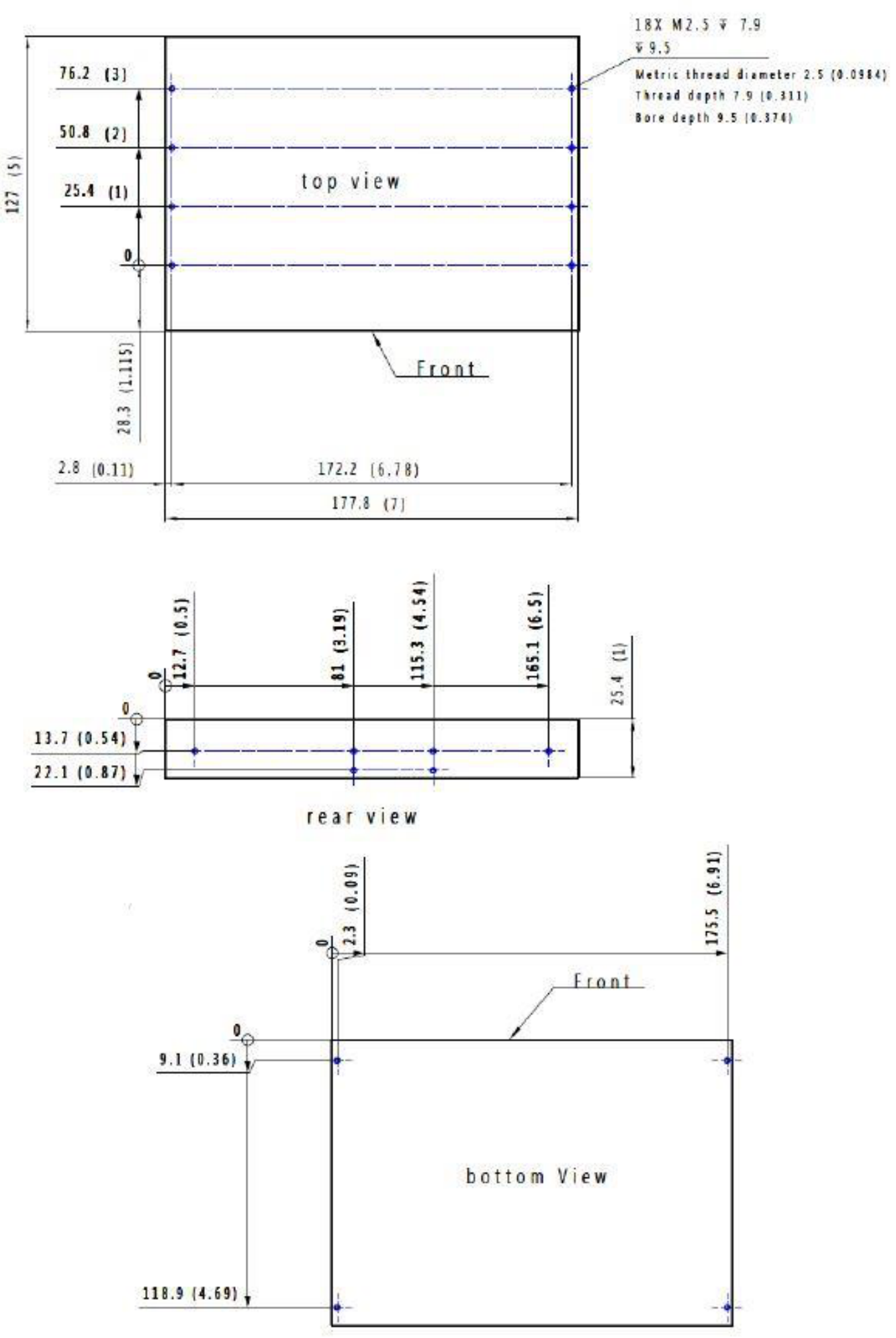
| Including connectors | W x L x H = 7 x 5.4 x 1 in |
| Excluding connectors | W x L x H = 7 x 5 x 1 in |
| Weight | < 2.4 lb |
Installation Instructions
The module relies on passive cooling. It is mandatory to mount the device on a heatsinking surface. Make sure the synthesizer operates under the conditions specified in this datasheet. Otherwise, the thermal protection will turn off the RF output.
12Interfaces
Front Panel

| Label | Type | Description |
|---|---|---|
| 1. DC IN | KPJX-4S | DC input (see also "Power Connector Assembly"). Redundant power supply input to the SPI Interface DC input (supply with higher voltage will be chosen). |
| 2. SPI | DF1BZ-20DP-2.5DS | SPI Interface, including DC input (see also "SPI Interface") |
| 3. ETH | RJ-45 | Ethernet port |
| 4. USB | Micro B | USB Port |
| 5. PULSE | SMA | Trigger / Pulse interface, 100 kΩ pull-up to +5.0 V |
| 6. PWR | LED | Power ON/OFF indicator |
| 7. REM | LED | Remote connection status indicator |
| 8. RF | LED | RF output ON/OFF indicator |
| 9. REF OUT | SMA | Reference signal output |
| 10. REF IN | SMA | Reference signal input |
| 11. RF OUT | SMA | RF output |
Power Connector Assembly
| Pin | Assignment |
|---|---|
| 1 | GND |
| 2 | DC Supply (see also "Power requirements") |
| 3 | GND |
| 4 | DC Supply (see also "Power requirements") |
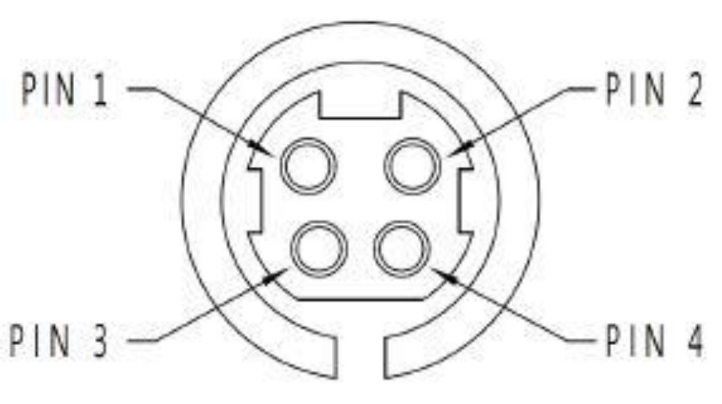
The power connector is a 4 pin, snap and lock receptacle. BNC recommends Kycon manufactured plugs KPPX-4P from its KPPX series.
SPI Interface
| Signal | Pin | Type | Description |
|---|---|---|---|
| SPI_CLK | 11 | Input | SPI clock. Supplied by the controlling host. The controlling host is the SPI master, the synthesizer is the SPI slave. |
| SPI_SS# | 13 | Input | SPI Slave Select. This signal is an active low input from the host to the synthesizer. It frames command communications. For each command, SPI_SS# goes low before the first bit is sent and goes high after the last bit is sent |
| SPI_MISO | 7 | Output | Master In/Slave Out. Data line from the synthesizer to the host. |
| SPI_MOSI | 9 | Input | Master Out/Slave In. Command/Data line from the host to the synthesizer. |
| TRIGGER | 17 | Input | Edge sensitive input. The trigger signal of +3.3 V can be configured for multiple trigger modes (see also "Trigger (PULSE)"). |
| LOCK | 15 | Output | Output indicates the RF output of the synthesizer is locked on its current setting (+3.3 V locked, 0 V unlocked). |
| REF_LOCK | 16 | Output | Output indicates the synthesizer has detected an external reference signal and locked on that signal (+3.3 V locked, 0 V unlocked). |
| RESET# | 18 | Input | Internally pulled up to +3.3 V with 100 kΩ resistor. Active low signal, which has a minimum width of 1 ms, will reset the synthesizer to a default state. |
| DC IN | 3, 4 | Input | External power supply (see also "Power requirements"). Redundant power supply input to the DC IN interface (supply with higher voltage will be chosen). |
| GND | 8, 10, 19, 20 | Ground. | |
| DNC | 1, 2, 5, 6, 12, 14 | Do not connect. Reserved for factory / future use. |
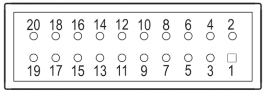
The SPI interface connector is a 20 pin, 2.50 mm spaced double-row header. BNC recommends HIROSE manufactured socket DF1B-20DS-2.5RC and corresponding contacts from its DF1B series.
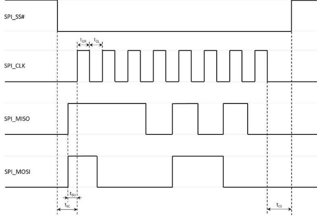
| Symbol | Value | Description |
|---|---|---|
| tSC | > 25 ns | SPI_SS# to be low before first clock edge |
| tCS | > 25 ns | SPI_CLK to be low before releasing SPI_SS# |
| tSU | > 15 ns | SPI_MISO/MOSI to be stable before rising edge of clock |
| tCH | > 25 ns | Minimum high time of a clock pulse |
| tCL | > 25 ns | Minimum low time of a clock pulse |
| fCLK | ≤ 12 MHz | Maximum clock frequency |
13Ordering Information
| Host Model | Product | Description |
|---|---|---|
| 805-SG | 805-SG-1 | 20 GHz wideband frequency synthesizer module (with AC adapter) |
| 805-SG | Option FS | Fast switching |
| 805-SG | Option 8K | Frequency Range extension to 8 kHz |
| 805-SG | Option PULSE | Internal / external pulse modulation |
For a configured quote or a demo unit, contact Berkeley Nucleonics.
14General Characteristics
| Parameter | Value |
|---|---|
| Remote programming interfaces | Ethernet, USB 2.0, SPI |
| Control language | SCPI Version 1999.0, native command set |
| DC power requirements | 12.0 – 30.0 VDC; 24 W typical |
| AC mains adapter (supplied) | 100-240 VAC in / 24 V, 2.7 A DC out |
| Storage temperature range | -40 to 70 °C |
| Operating temperature range | 0 to 60 °C, non-condensing, temperature of passive heatsink |
| Operating and storage altitude | up to 15,000 feet |
| Safety/EMC |  Complies with applicable Safety and EMC regulations and directives Complies with applicable Safety and EMC regulations and directives |
| Recommended calibration cycle | 24 months |
15Applications
- QuickSyn FSW-0010 / 0020 replacement
- Automated Test Environment
- Characterizing antennas, semiconductor devices, and other components
- Radar signal generation and Electronic warfare
Berkeley Nucleonics Corporation · info@berkeleynucleonics.com · 800-234-7858
Cited in peer-reviewed research
Independent publications citing this instrument, indexed by Bioz. Citation counts and Bioz Stars ratings are shown live and update as new papers are indexed.