Electro-Optic Modulation & Detector Gating
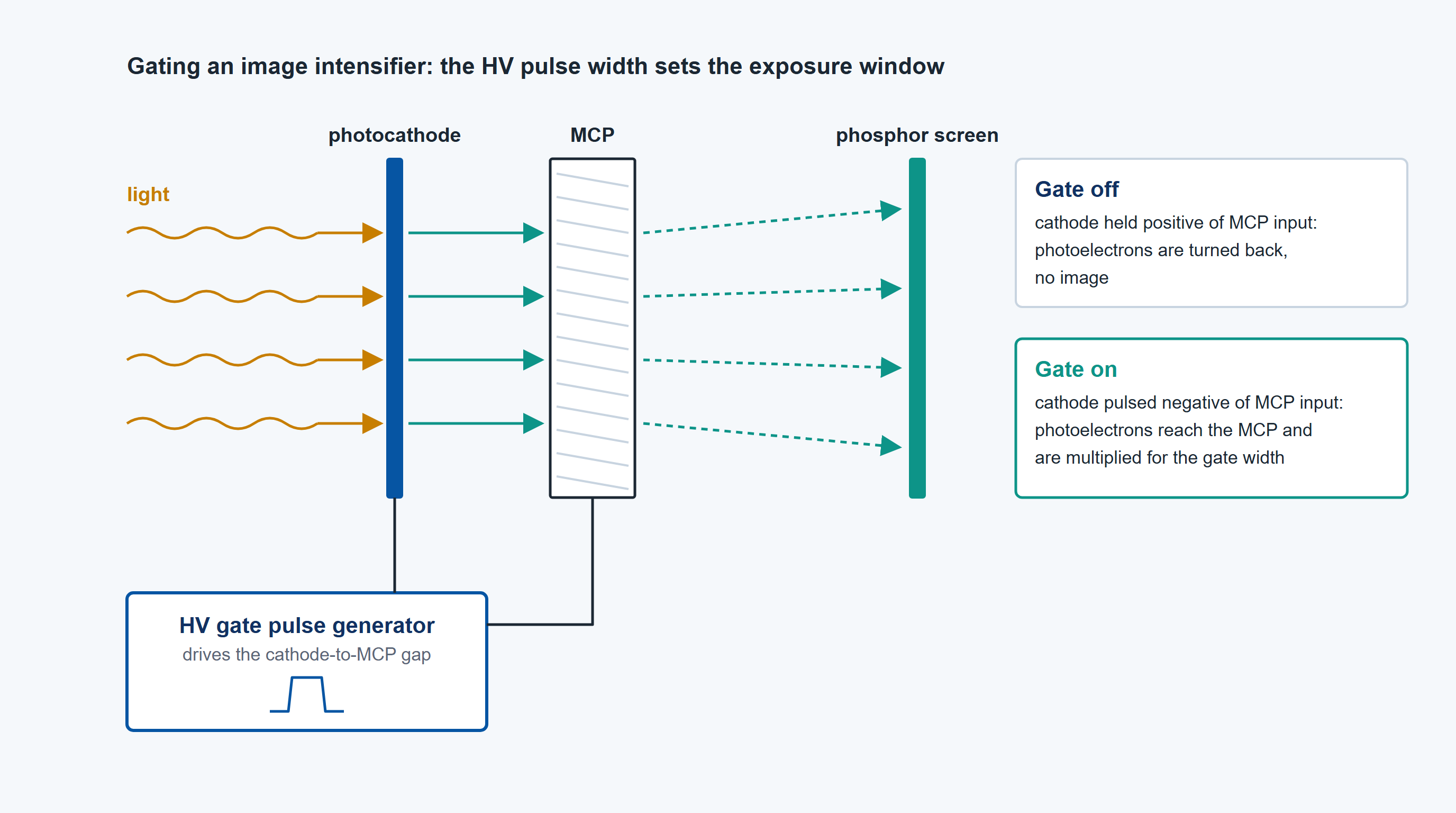
Time-resolved detection often depends on turning a detector on for a narrow window and off the rest of the time. Gating a microchannel plate, a photomultiplier tube, or an image intensifier means pulsing its bias so it amplifies only during a chosen interval, which suppresses background, isolates a signal in time, and protects the device from light that would otherwise overwhelm or damage it. The same fast HV pulsing drives the deflection plates and electro-optic modulators that chop, sweep, or shutter a beam. In all of these, the gate is only as good as the high-voltage pulse that defines it.
The detector electrode is a capacitive load, and the gate is a high-voltage pulse with a controlled width, fast leading and trailing edges, and a clean shape. The width sets the time window (Figure 1), the edges set how sharply the detector opens and closes, and the cleanliness of the pulse determines whether the gate adds artifacts to the very measurement it is meant to isolate. A pulser built for this job has to deliver all three at once, repeatably, into a load that resists fast transitions.
The Challenge
Gate-width control is the first requirement. The detector should be active for exactly the intended interval, which can range from tens of nanoseconds to microseconds, and the width must be settable and stable shot to shot. A gate that drifts in width changes the collected signal from one acquisition to the next, which corrupts time-resolved data. The leading and trailing edges have to be fast relative to the gate, otherwise the open and close are smeared and the effective window is blurred at both ends.
Fast, clean on and off transitions are the second requirement, and they are demanding because the detector bias is capacitive. Driving an MCP or PMT bias network quickly takes real current, and the edges must be fast without overshoot, because overshoot on a detector bias can spill gain outside the intended window or stress the device. The trailing edge matters as much as the leading one: a slow or ringing turn-off lets the detector respond to light it should have ignored.
Protecting the detector is the third requirement. MCPs, PMTs, and image intensifiers are expensive and can be damaged: an uncontrolled pulse, an overshoot, a wrong polarity, or a fault on the output can degrade or destroy them. The pulser has to be well-behaved at its edges and predictable under fault, so the device it gates sees only transitions within its ratings.
The BNC Approach
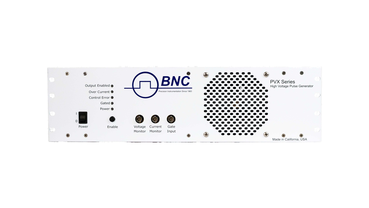
DEI pulse generators gate capacitive detector loads with a half-bridge (totem-pole) output that drives the load actively in both directions, so the gate opens and closes with equally fast edges. On the PVX-4141 the output switches between two user-supplied DC supplies, VHigh and VLow, that set the off-state and on-state bias directly, and the TTL gate sets the width. Its front-panel voltage and current monitors let the engineer see the gate on the detector bias, check the width and the edges, and watch for overshoot before a detector is connected. The PVM-4210 and PVM-1001 modules have no monitor outputs; observe their output with a suitably rated high-voltage probe during setup.
The models below cover gate amplitudes from 50 V (the lowest specified level of the PVM-1001) to 3,500 V (PVX-4141), and repetition from single shot to 1 MHz continuous (PVM-1001), with 5 MHz bursts on the PVM-1001 and PVM-4210. Over-current shutdown on the PVX-4141 and PVM-4210 protects the output against arcs and shorts at the load.
Recommended Instruments
For higher-voltage MCP and image-intensifier gating, the PVX-4141 delivers up to 3,500 V with rise and fall of 25 ns or less into 50 pF, a 60 ns minimum gate width, jitter under 200 ps, and single shot to 30 kHz continuous at 3,500 V. Where the gate voltage is moderate, the PVM-4210 provides a +950 V and a −950 V output that pulse together for a 1,900 V differential swing, with rise and fall of 25 ns or less, minimum width under 50 ns (FWHM), jitter under 1 ns, and single shot to more than 20 kHz continuous with 5 MHz bursts. Each channel amplitude is set from 0 to 950 V on the module.
For narrow gates into a 50 ohm terminated input, the PVM-1001 switches an external supply of up to 950 V to its output with a rise time of 8 ns or less (PVM-1001-P, 200 V to 950 V) and gate widths from 55 ns to 10 µs, at up to 1 MHz continuous and 5 MHz in burst. It is specified into a 50 ohm resistive load, and its fall time is longer than its rise: up to 50 ns at 450 V to 950 V and up to 130 ns at 50 V to 199 V, so the closing edge sets the shortest clean gate. Positive and negative outputs are separate models, PVM-1001-P and PVM-1001-N. Electro-optic modulator and Pockels-cell drive is covered in the Pockels cell and Q-switch brief. The right model follows from the detector bias voltage, the load (a capacitive electrode or a terminated 50 ohm input), the gate width, and how fast both edges must be relative to that width.
Confirm the gate polarity, the off-state and on-state voltages, and the edge behavior against your detector ratings before applying any pulse. On the PVX-4141 the built-in monitors show the gate on a scope before it reaches the MCP, PMT, or intensifier. An applications engineer can review the gate against your detector limits.
Getting Started
Begin with the detector: its bias voltage, its capacitance, the gate width your measurement requires, and how fast the edges must be to define that window cleanly. Note the repetition rate and any protection limits that constrain the pulse. Those parameters select the model and set the rise-time and width targets. On the PVX-4141 the VHigh/VLow inputs map onto the off-then-on gating a detector needs, and its monitors show the gate before it reaches the detector.
Talk to a BNC applications engineer at info@berkeleynucleonics.com or 800-234-7858. Bring your detector bias, gate width, edge requirement, and repetition rate, and we will match a DEI pulse generator to a gate that protects your detector and isolates your signal.