Pockels Cell & Q-Switch Driving
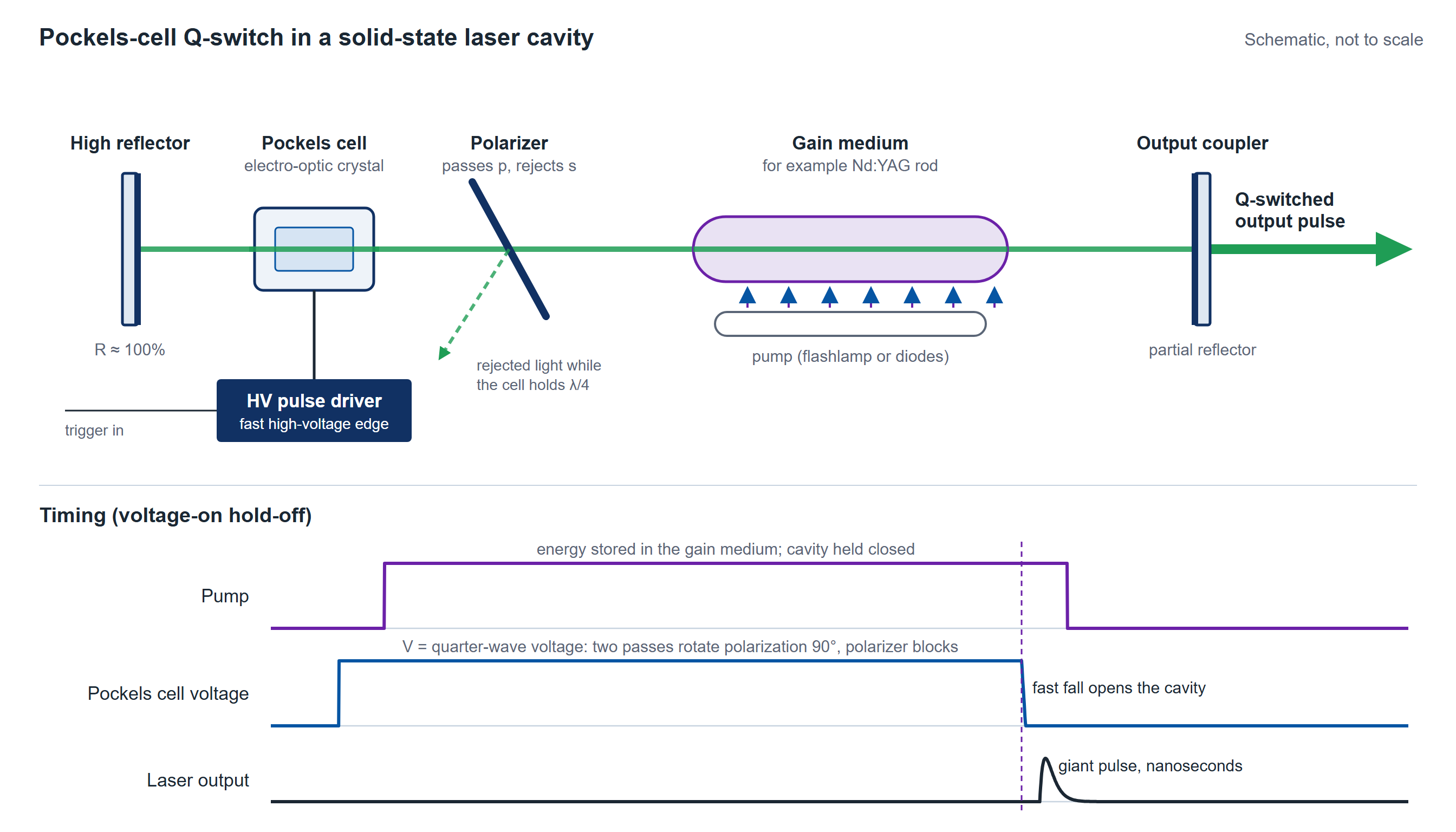
A Pockels cell is an electro-optic crystal whose polarization response changes with applied voltage. Place one inside a laser cavity, hold it at the right potential, and it becomes a fast optical switch: the cavity can be held below threshold while energy builds in the gain medium, then switched open in nanoseconds to dump a giant pulse. That is the heart of active Q-switching and cavity dumping, and the quality of the optical pulse is set almost entirely by the quality of the high-voltage pulse that drives the crystal.
The crystal presents a small capacitance to the driver, typically a few to tens of picofarads. Switching it means moving kilovolts across that capacitance in nanoseconds, which takes amperes of peak current (Figure 1), at a set instant relative to the pump and the cavity. The driver therefore has to deliver a fast high-voltage edge into a capacitive load with low jitter, because in a Q-switched cavity the timing of the switch sets the timing and the energy of the emitted pulse.
The Challenge
Rise time is the first constraint, and it couples directly to cavity timing. In Q-switching, the cell has to switch in a time short compared with the build-up of the giant pulse; a slower transition lets the pulse start to build while the cell is only partly switched, which lowers the peak power and lengthens the pulse. Cavity dumping is tighter: the transition has to be comparable to or shorter than the cavity round trip, 2L/c, which is 5 ns for a 0.75 m cavity and 20 ns for a 3 m cavity.
Jitter is the second constraint, and it is where cavity dumping is most demanding. Dumping requires the switch to fire at a precise moment in the intracavity build-up, and any shot-to-shot variation in that moment translates into variation in output energy and timing. For systems that synchronize the laser to an external event, an amplifier chain, a probe pulse, a machine clock, low jitter between the trigger and the HV edge is what makes the laser usable as a timed source rather than a free-running one.
Repeatability ties the two together. A driver that produces a slightly different edge or delay on each shot makes every optical pulse slightly different, which matters in precision machining, ranging and scientific work. Overshoot or ringing after the edge modulates the retardation of the cell, so the settled level after the transition matters as much as the speed of the transition.
The BNC Approach
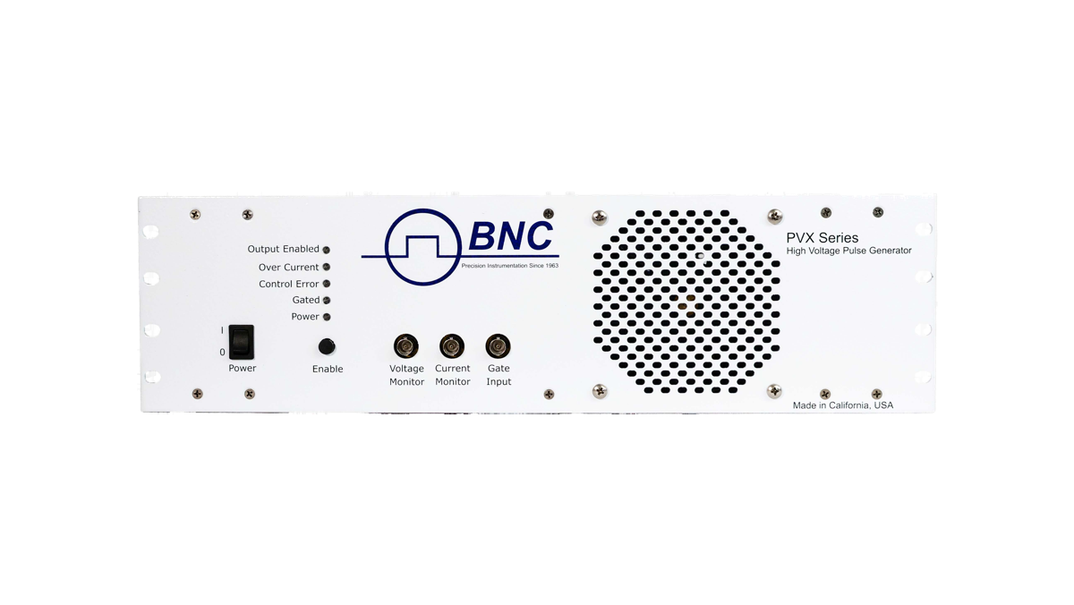
The DEI PVX pulse generators are built for this load: a small capacitance that needs a fast kilovolt transition placed precisely in time. The half-bridge (totem-pole) output drives the crystal actively in both directions, so the edge that opens the switch and the edge that closes it are equally fast, with over/undershoot under 5 percent. The output switches between two user-supplied DC supplies, VHigh and VLow: the cell rests at one level, for example the quarter-wave voltage that holds a Q-switched cavity closed, and switches to the other for the width of the gate. The TTL gate sets pulse width and repetition rate; the supplies set amplitude.
Shot-to-shot jitter is under 200 ps on the PVX-4141 and under 1 ns on the PVX-4130 and PVX-4151, which suits these drivers to synchronized Q-switching. Front-panel voltage and current monitors (1000:1 into 1 MΩ and 10 A/V into 50 Ω on the PVX-4141) let the laser engineer observe the edge into the real crystal, check the switching level, and confirm that the top has settled before the optical pulse is generated.
Recommended Instruments
The PVX-4141 is the default for Pockels-cell and Q-switch driving: output to 3,500 V, rise and fall time of 25 ns or less, jitter under 200 ps shot to shot, and single shot to 30 kHz continuous at 3,500 V, all specified into a 50 pF load through 6 ft of RG-59 cable. At lower load capacitance or voltage it runs continuously to 400 kHz. For cells that need a higher switching voltage, the PVX-4130 extends the same capacitive-load design to ±6,000 V, with rise time under 60 ns (about 45 ns at 6,000 V), jitter under 1 ns, and single shot to 10 kHz.
For cells with a lower switching voltage at a high repetition rate, the PVX-4151, the current production version of the PVX-4150, delivers 1,500 V with rise and fall under 25 ns (under 20 ns typical) and jitter under 1 ns, from single shot to 240 kHz continuous at 1,500 V and 5 MHz in burst. Where the cell can be driven differentially, the PVM-4210 module puts +950 V and −950 V on the two electrodes at once, a 1,900 V differential swing, with rise and fall of 25 ns or less, built-in high-voltage supplies, and single shot to more than 20 kHz continuous. The choice follows from the half-wave or quarter-wave voltage of the crystal, its capacitance with the cable, the cavity timing and the repetition rate. A 20 to 25 ns edge suits Q-switching and the dumping of cavities with a round trip of about that length or longer; dumping a cavity with a round trip of a few nanoseconds needs a faster driver than the models listed here.
Compare the driver rise time against your cavity round-trip and required hold-off. A faster edge generally yields a cleaner dumped pulse, but the crystal capacitance sets how much current the driver must source to achieve it. An applications engineer can balance edge, voltage, and rate for your cavity.
Getting Started
Begin with the crystal: its half-wave or quarter-wave voltage, its capacitance, and the polarity of the bias your cavity uses. Add the cavity timing requirement (the round-trip time and, for dumping, the build-up window) and the repetition rate. Those values select the model and set the rise-time and jitter targets. On the PVX models the VHigh/VLow supply inputs map onto the bias-then-switch operation of a Pockels cell, and the front-panel monitors show the switching edge into your crystal during bring-up.
Talk to a BNC applications engineer at info@berkeleynucleonics.com or 800-234-7858. Bring your crystal capacitance, half-wave voltage, cavity timing, and repetition rate, and we will match a DEI pulse generator to the switching precision your laser requires.