1Introduction
This note describes how the Serial Pattern Generator (SPG) mode of the Model 675 and Model 685 Arbitrary Waveform Generators produces the signals needed to test and characterize standard logic gates and other digital circuits. The SPG combines pulse and edge shaping with a programmed multilevel pattern, so one channel reproduces the levels and transitions a real logic signal carries. With up to 12 Vpp into 50 ohms (24 Vpp into an open circuit) and a baseline offset of ±6 V into 50 ohms (±12 V open) on the Model 675 with its high-voltage option, and symbol rates to 300 Mbaud on the Model 675 and 1.5 Gbaud on the Model 685, the instruments take the place of a legacy pulse generator in this work.
| Key Issues | Characterize digital logic gates and integrated circuits. |
|---|---|
| Solutions | Model 675 or Model 685 Arbitrary Waveform Generator in SPG mode; a four-channel oscilloscope with bandwidth well above the pattern rate. |
| Results | Accelerate research, reliability, and failure analysis studies of semiconductor devices. Reduce the time from setup to running characterization of digital logic gates. |
2Model 675 & 685 SPG Key Features
Up to 4 logic levels
Each channel can define up to 4 independent voltage levels and emulate, in addition to logical ‘0’ and ‘1’, a tristate buffer or a weak ‘0’ signal when a bus is not driven.

Edge Definition
The shape of each transition between the levels can be arbitrarily defined by the user. This feature is capable of shaping the edge as RC transient, or to add a positive overshoot. The Model 675 has 16-bit vertical resolution and 400 MHz bandwidth; the Model 685 has 16-bit resolution with transition times as short as 400 ps (10 to 90 percent).
Amplitude
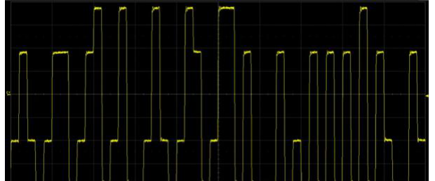
The Model 675 reaches 6 Vpp into 50 ohms as standard and 12 Vpp with its high-voltage option (24 Vpp into an open circuit), and a programmable baseline offset shifts the window by up to ±3 V into 50 ohms as standard, ±6 V with the option (±12 V open). With the offset, the Model 675 generates a 0 to 12 V signal into 50 ohms (0 to 24 V open). The Model 685 covers 0 to 5 Vpp into 50 ohms with a ±2.5 V hardware offset, which spans the 3.3 V and 5 V logic families. Figure 2 shows a four-level pattern on an oscilloscope.
Multi-Instrument synchronization up to 32 channels
A Model 685 has up to 8 analog channels, and up to four units synchronize over a dedicated bus to build a 32-channel system.
Fine time resolution
Channel-to-channel skew is adjustable in steps of 5 ps on the Model 675 and 100 fs on the Model 685.
Generation
- Continuous: the generation starts when the user presses the Start button and it ends when the user presses the stop button.
- Burst: the instrument waits for a trigger and then the pattern is generated for the selected number of times. At the end of the burst the instrument waits for a new trigger.
- Modulation: the instrument applies an AM, FM, PM, FSK or PSK modulation to the generated pattern.
Selectable Header
The Model 675 pattern memory holds up to 2 Mbit for two-level patterns (1 Msymbol for three or four levels) and the Model 685 up to 2 Msymbols. An initial part of the pattern can be generated once while the rest repeats.
Intuitive User Interface
The instrument is programmed from its touch screen and keyboard (Figure 3). In an automated test bench, an external controller drives it with SCPI commands.

3Standard Logic
Standard logic gates are the basic blocks of every digital circuit. Programmable devices such as microcontrollers (MCUs) and programmable gate arrays carry most of the logic in a modern design, yet discrete gates still have a place: where a function cannot be realized in the programmable device, where the design is too simple to justify one, where an external gate is needed to reach a bit rate the programmable device cannot support, where a level shifter joins devices with different voltage standards, or where a multiplexer extends the pin count of an MCU (Figure 4).
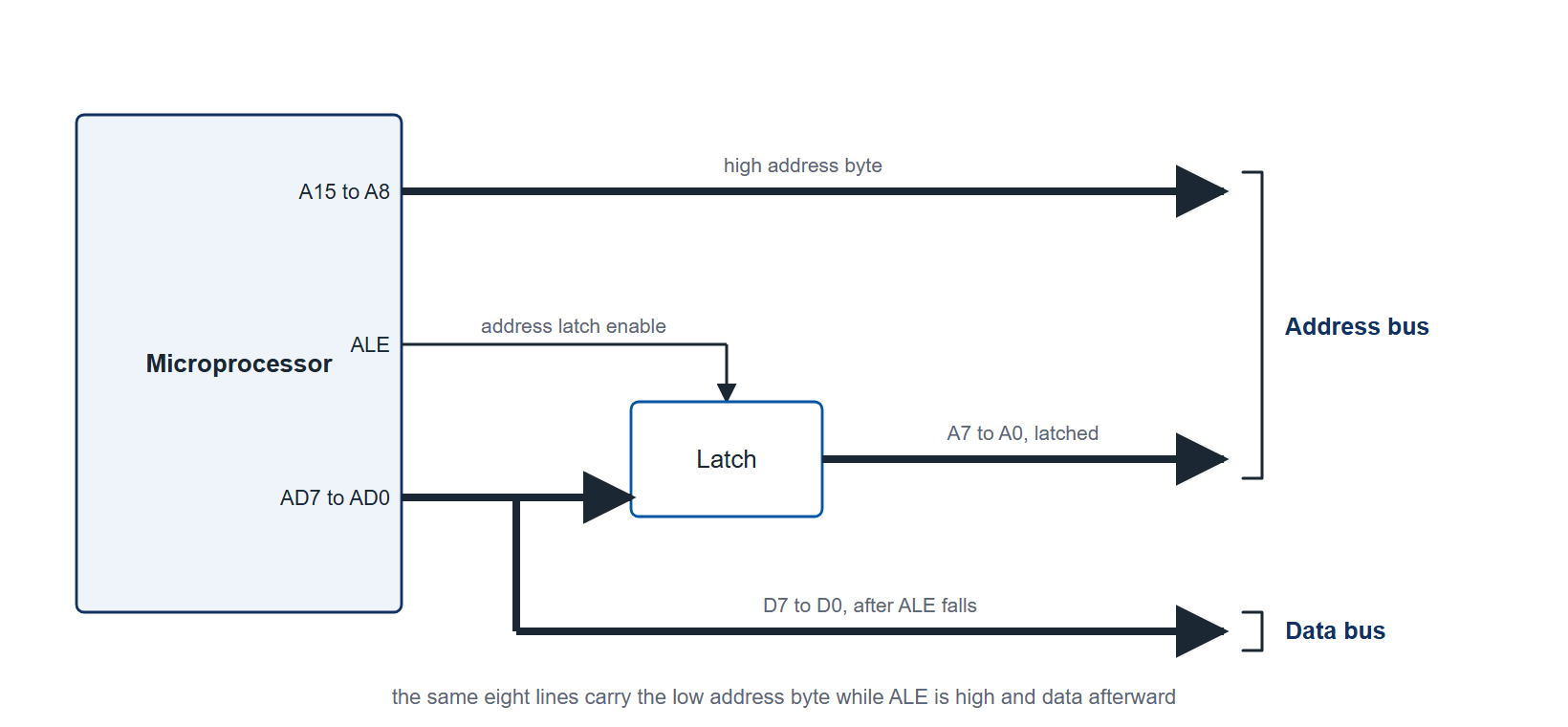
Devices from different logic families (TTL, CMOS, BiCMOS and others) share the same logical functions. To characterize and test them, from single gates (NOT, NAND, NOR) to multichannel latches and counters, the test signals need defined edge shapes, overshoot and amplitude. Real digital signals are not ideal: they take time to switch and can carry overshoot, so the most informative test signal is an analog one whose edge shape, amplitude and overshoot are set by the user.
For these tests the SPG combines the digital pattern with the analog characteristics of the front end: edge shaping, amplitude, noise, and modulation.
The sections that follow show how to generate the signals for two tests on a three-input AND gate.
4A. Measurement of the Propagation Delay of Asynchronous Logic Gate
The application below considers a three-input AND gate (Figure 5), and the principle holds for any logic network. The three inputs of the gate are logically equivalent, but analog characteristics such as propagation delay depend on the internal architecture.

With the SPG, the user defines the analog characteristics of the signal on each input of the gate under test, setting the voltage levels and the edge shape independently per channel.
Figure 6 shows the connections for this test:
- The 1st, 2nd and 3rd channels of the pattern generator are connected to the input of the AND gate.
- The 4th channel is connected to oscilloscope as reference.
- The Output of the AND gate is connected to the oscilloscope.
- For simplicity, the power supply, ground, and other components needed for the gate’s operation are omitted.

How to configure the Pattern Generator using the software interface
1. From the “Carrier Data” tab, set the level number to 2, define the symbol period and select Custom as the pattern mode (Figure 7).

2. From the “Transition Data” tab, define the shape of each edge and the voltage of each level (Figure 8). In the screens shown the transitions are linear ramps of 1.5 ns between 0 and 5 V; the tests in section B use 4 ns and 7 ns edges.

3. Definition of the pattern:
| Ch 1 | 01111111 |
|---|---|
| Ch 2 | 01111111 |
| Ch 3 | 00011110 |
| Ch 4 | 00011110 |
| Ch 5 – 8 | not used |
To evaluate the propagation delay of input 3, inputs 1 and 2 go high at the same time; once they are stable, input 3 rises, stays high for four symbols, then falls. Channel 4 carries the same pattern as channel 3 and is the oscilloscope reference (Figure 9). The pattern is loaded through the import dialog (Figure 10).
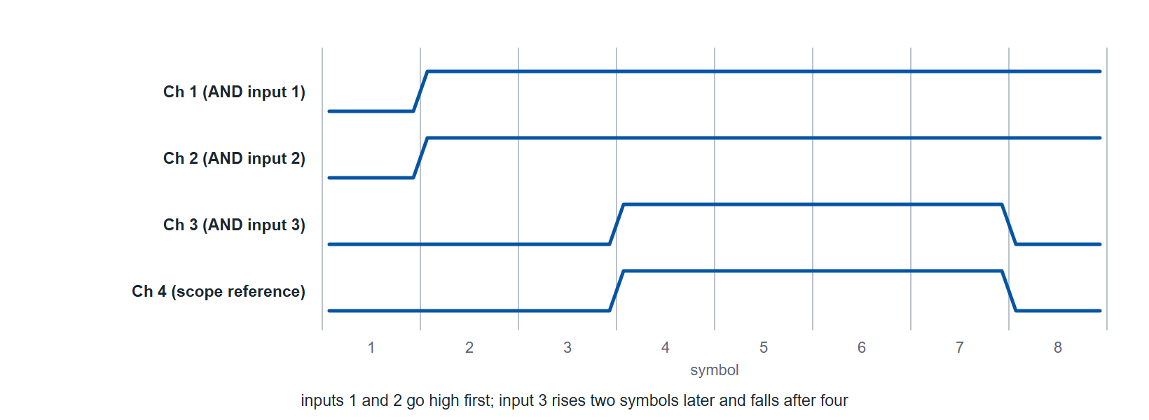

4. Press the Run button and observe the result (Figure 11).

Figure 11 shows the delay between the gate output and SPG channel 4.
Note: to compensate for the delay of the cables the user can adjust the initial delay of channel 4. This setup is useful in characterizing the input-to-output propagation delay for input 3, but by changing the pattern the user can also observe the behavior of other inputs.
5B. Effects of Simultaneous Switches in Asynchronous Logic
With asynchronous logic, the behavior of a gate when two or more inputs switch at the same instant is worth measuring. Starting from the previous setup, this example tests what happens when input 1 goes high at the instant input 2 goes low.
The following pattern was loaded:
| Ch 1 | 11000011 |
|---|---|
| Ch 2 | 00111100 |
| Ch 3 | 11111111 |
| Ch 4 – 8 | not used |
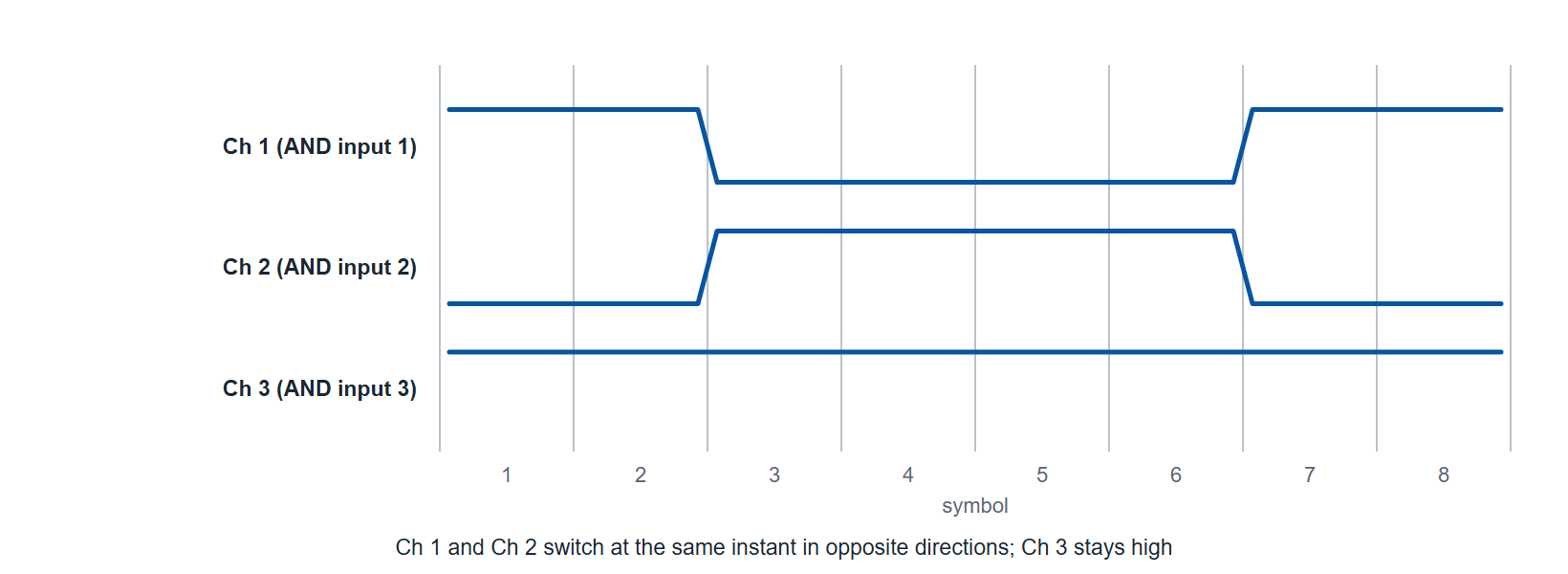
Logically the output should stay at 0, but depending on the input edges and the gate’s internal architecture a spike can appear on the output. Figure 13 shows two spikes at the input transitions.

Figures 14 and 15 come from the same setup with the rise and fall times and the channel skew varied.
- Skew channel 1 – 2: 2 ns
- Rise / Fall time: 4 ns

With 2 ns of skew between channels 1 and 2, a spike appears when input 1 switches high (Figure 14).
- Skew channel 1 – 2: 0
- Ch 1 Rise time 7 ns
- Ch 1 Fall time 4 ns
- Ch 2 Rise time 7 ns
- Ch 2 Fall time 4 ns

With no skew and a 7 ns rise time against a 4 ns fall time, no spike is recorded (Figure 15).
6Conclusion
In SPG mode the Model 675 and Model 685 give a designer multiple outputs, a wide voltage window, custom and modulated patterns, and user-defined transition shapes for characterizing digital devices. The touch-screen interface and SCPI control shorten the path from setup to measurement.
7About Us
Berkeley Nucleonics Corporation (BNC) has designed and built precision electronic instrumentation for test, measurement, and nuclear research since 1963. Our corporate headquarters are in San Rafael, California, with additional manufacturing facilities and sales offices located throughout the United States.
Contact Information
Berkeley Nucleonics
2955 Kerner Boulevard
San Rafael, CA 94901
info@berkeleynucleonics.com or 800-234-7858
Product videos and tutorials are on the Berkeley Nucleonics YouTube channel.