The first edition of this book contained an appendix titled New Materials that introduced GAGG:Ce and CLLBC. Both are now standard catalog items rather than novelties. This appendix is the second-edition update: a deep dive on the materials that are new since 2023, the materials that have moved through commercial scaling between editions, and the materials that are research-stage but worth tracking.
The structure follows the order in which an applications engineer is likely to evaluate the materials: established advances first, then commercial-scaling updates, then research-stage materials.
Cs2HfCl6, sometimes written as CHC in the literature, is the most consequential new scintillator since GAGG:Ce reached commercial scale. The material was first characterized as a scintillator in the mid-2010s [1], reached commercial-quality crystal sizes around 2022, and is now appearing in catalog detector configurations.
Physical properties. Density 3.86 g/cc. Cubic crystal structure (K2PtCl6 type). Melting point around 820 C. Non-hygroscopic, which is the headline property and the reason CHC matters. The material can be packaged in plastic or epoxy housings rather than welded metal canisters, which simplifies low-cost detector packaging dramatically.
Scintillation properties. Emission peak at 380 nm, well matched to standard bialkali PMTs and to NUV-optimized SiPMs. Decay time around 4 microseconds (slow for a high-resolution scintillator, which limits high-rate applications). Light yield reported at 130 to 180 percent of NaI(Tl) in research-grade samples [1][2]. Energy resolution at 662 keV: 2 to 3 percent FWHM in commercial samples, with sub-1 percent reported in best research samples [1]. The non-proportionality is excellent, comparable to or better than LaBr3:Ce.
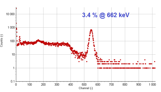
The headline number. Yoshikawa et al. at SCINT 2024 reported 0.9 percent FWHM at 662 keV from a 10 mm by 10 mm by 5 mm Cs2HfCl6 sample read out by a NUV-HD SiPM array. This is competitive with small high-purity germanium detectors at the same energy and is the best room-temperature scintillator energy resolution ever reported. The result has been corroborated by independent measurements at other groups [3].
Where CHC stands in 2026. Crystal-growth scaling is the binding constraint. Commercial samples are available up to roughly 30 mm by 30 mm by 30 mm; growth of larger boules is in progress. Lead time is several months. The material is not a drop-in replacement for NaI(Tl) at large volume yet. Where it shines is in compact spectroscopy: small handheld instruments, portable isotope identifiers, low-rate spectrometry where the slow decay does not hurt.
Applications profile. Strong fit for: handheld isotope identification (HALEU and SNM verification), low-background spectrometry where La-138 background of LaBr3:Ce is a problem, ruggedized field instruments where the non-hygroscopicity simplifies packaging. Weak fit for: high-rate counting (4 microsecond decay), large-volume gamma area monitoring (lead time and crystal size), fast timing.
Outlook. As crystal growth scales, CHC will displace LaBr3:Ce in handheld instruments where the La-138 background matters and will compete directly with LYSO and CsI(Tl) in some compact applications. The 2030 catalog will likely treat CHC as a standard material.
Going Deeper - Why Cs2HfCl6 has high light yield
The high light yield of CHC traces to the dominant emission mechanism: a self-trapped exciton on the [HfCl6]^2- octahedron. Unlike doped scintillators (NaI(Tl), CsI(Tl), LaBr3:Ce) where the activator concentration is a few percent at most, the emission center in CHC is the host structural unit itself, present at 100 percent concentration. The result is a high probability that exciton energy migrates to a recombination center and is converted to scintillation light, with relatively few competing non-radiative paths. The trade-off is the slow decay (microseconds versus tens of nanoseconds for cerium-doped materials), because the self-trapped exciton's radiative lifetime is intrinsically long. The same physics applies to other "intrinsic" scintillators (BGO, CdWO4) which also have slow decay.
GAGG:Ce reached commercial scale in the mid-2010s and is now a standard high-light-yield, fast, non-hygroscopic gamma scintillator. The garnet family has expanded substantially since then. The variations cluster into three categories.
GAGG:Ce in its single-doped form has a decay time of 90 to 150 nanoseconds with a substantial slow component. Magnesium codoping (GAGG:Ce,Mg) shortens the decay to 50 to 90 nanoseconds by suppressing the slow component, with a modest light yield reduction [4]. The faster decay matters for high-rate applications and for timing applications.
Other codopants have been investigated. Calcium codoping has been reported to improve scintillation yield further but with longer decay times than magnesium codoping. Boron codoping has been studied as an alternative non-radiative-suppressor [5].
The state of the field in 2026: GAGG:Ce,Mg is commercially available and is preferred for new high-rate applications. Single-doped GAGG:Ce remains in production for applications where the faster decay is not needed.
Compositional substitutions in the garnet host change scintillation properties without altering the activator. The substitutions that have been characterized and produced commercially:
GYAGG:Ce (Gd,Y)3(Al,Ga)5O12:Ce. Substituting yttrium for gadolinium reduces density slightly (5.8 g/cc vs. 6.63 g/cc for GAGG) and reduces self-absorption issues that limit bulk crystal sizes in high-Gd materials. Light yield 110 to 130 percent of NaI(Tl). Used in applications where large-volume garnet is needed and the slight density reduction is acceptable.
LuAG:Ce (Lu3Al5O12:Ce). Lutetium-based garnet. Higher density (6.73 g/cc) and Z than GAGG. Lower light yield (50 to 60 percent of NaI(Tl)). Used in fast-timing PET and in applications where stopping power matters more than light yield.
LuAG:Pr (Lu3Al5O12:Pr). Praseodymium-doped variant of LuAG. Decay time around 20 nanoseconds, the fastest in the garnet family. Emission at 305 nanometers requires a UV-transmissive window or a SiPM with substantial NUV PDE. Used in fast-timing and high-rate applications where the deep-UV emission is acceptable.
The newest development in the family is the production of garnet scintillators not as Czochralski-grown single crystals but as transparent polycrystalline ceramics, fabricated by powder consolidation and high-pressure sintering. The technique allows fabrication of complex shapes (pixel arrays, fibers, large flat panels) that would be difficult or impossible as single crystals, and it eliminates the slow Czochralski growth step that constrains single-crystal lead times.
Transparent ceramic garnets reported in the literature include LuAG:Ce, GAGG:Ce, GYAGG:Ce, and YAG:Ce variants [6][7]. Performance approaches but does not yet match the best single-crystal samples at the same composition. Energy resolution is typically 5 to 7 percent at 662 keV, with substantial sample-to-sample variation. The technique is being driven by demand for high-volume PET arrays and for industrial radiography panels.
Outlook. Transparent ceramic garnets will not replace single-crystal scintillators across the board, but they will fill the gap where complex geometry or large area is needed. SCINT 2024 sessions on ceramic scintillators were the most heavily attended of the conference, and IEEE NSS-MIC 2024 included a dedicated workshop on the topic.
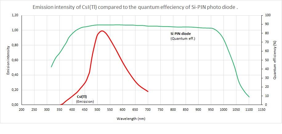
CsI(Tl) is not a new scintillator. It has been used since the 1950s. The new material story is the systematic optimization of CsI(Tl) for SiPM readout, which has produced detector performance that no PMT-coupled CsI(Tl) configuration achieves.
The combination matters because:
The optimization questions that have been worked through in the SCINT and IEEE NSS literature [8][9][10]:
SiPM cell pitch. Smaller cells (10 to 20 micrometer pitch) give higher dynamic range (more cells means less saturation per scintillation event) but lower fill factor and lower PDE. Larger cells (35 to 50 micrometer pitch) give higher PDE but saturate at large pulses. The sweet spot for CsI(Tl) at gamma energies up to several MeV is 25 to 35 micrometer pitch.
Array tiling and gap minimization. Multi-channel SiPM arrays for large crystal faces leave dead space between channels. Tiling arrays with sub-millimeter dead gaps and reading them out with summing electronics or with multi-channel digital pulse processors recovers most of the light that would otherwise be lost.
Optical coupling. Air-gap coupling is simpler and avoids potting compounds that could outgas in vacuum, but loses about 20 percent at the crystal-air interface. Index-matched silicone rubber pads with refractive index 1.4 to 1.5 give 90 percent or better coupling efficiency, are reworkable, and tolerate thermal cycling better than cured optical cement.
Diffuse reflector versus specular reflector. Diffuse reflectors (Teflon tape, ESR film) randomize photon paths and are tolerant of crystal-surface imperfections. Specular reflectors (aluminized mylar, dielectric stacks) preserve photon directionality and can give higher coupling to a small SiPM array, at the cost of greater sensitivity to surface defects. Diffuse reflectors dominate in commercial CsI(Tl)+SiPM detectors.
Crystal surface treatment. CsI(Tl) surface finish (polished versus matte, treatment for moisture resistance) substantially affects light extraction. A polished crystal with a high-quality reflector can give 10 to 15 percent more light at the SiPM than a matte-finish version of the same crystal.
Temperature compensation. Active SiPM bias compensation (Section 7.3) keeps gain stable to within 1 percent over a 50 C temperature range. This is the engineering enabler that makes CsI(Tl)+SiPM detectors viable for outdoor and field use.
The performance achievable with optimized CsI(Tl)+SiPM at room temperature: 6 to 7 percent FWHM at 662 keV for a 1-inch by 1-inch crystal, comparable to the best NaI(Tl)+PMT configurations of the same volume. For larger crystals (3-inch by 3-inch and above) the comparison shifts toward NaI(Tl)+PMT being competitive on a per-unit-area basis, because the SiPM array cost grows with area while a PMT photocathode area is set by the tube neck size.
SrI2(Eu) was introduced in the first edition. Crystal growth and energy resolution have continued to improve.
State in 2026. Commercial samples up to roughly 40 mm by 40 mm by 40 mm are available. Energy resolution at 662 keV in best samples is 2.5 to 2.7 percent FWHM, comparable to LaBr3:Ce. The slow decay (1 to 5 microseconds) limits SrI2(Eu) to moderate-rate applications. Hygroscopicity is severe; packaging must be hermetic.
Where SrI2(Eu) wins over LaBr3:Ce. No intrinsic background. Lower cost per gram in some supply situations. Slightly better non-proportionality at low energies (below 100 keV).
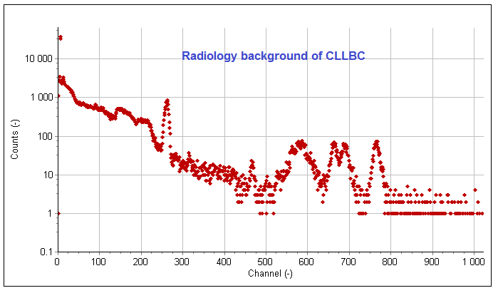
Where SrI2(Eu) loses. Slower decay limits rate. Hygroscopicity is comparable, not better. La-138 background of LaBr3:Ce is increasingly addressed in commercial detectors by using thinner internal shielding and the lower lanthanum-content variants (LBC), reducing the relative advantage of SrI2(Eu).
Outlook. SrI2(Eu) will retain a niche in low-background spectrometry and in applications where the lowered cost and good resolution win, but it is not displacing LaBr3:Ce or CHC across the board.
The elpasolite family was introduced in the first edition. The materials have moved from research curiosities to standard catalog items in homeland-security and physics applications.
CLYC (Cs2LiYCl6:Ce). Density 3.31 g/cc. Decay components 1, 50, 1000 ns. Light yield 30 to 40 percent of NaI(Tl) for gamma. Energy resolution 5 to 6 percent FWHM at 662 keV. Hygroscopic. The PSD figure of merit is 2.5 to 3.5 in commercial samples. CLYC is the older and more widely deployed of the family.
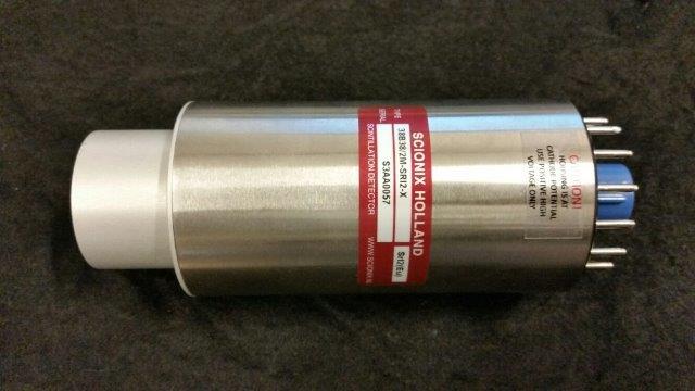
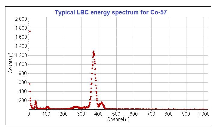
CLLB and CLLBC. CLLB is Cs2LiLaBr6:Ce. CLLBC is the mixed Cs2LiLa(Br,Cl)6:Ce. Both have density around 4.1 g/cc, light yield 60 to 70 percent of NaI(Tl) for gamma, and PSD FoM above 3 in commercial samples [11]. Energy resolution at 662 keV is 4 to 5 percent FWHM in CLLBC. The improved light yield over CLYC translates to better gamma spectroscopy at the same crystal volume, and CLLBC has displaced CLYC in many new handheld designs.
Crystal sizes. Commercial samples up to 1.5 inch by 1.5 inch are routine; 3-inch by 3-inch is available in CLLBC with longer lead times. Larger sizes are in development but remain expensive.
Outlook. Elpasolites are mature commercial materials. Future developments are likely to be incremental: better PSD, lower-cost crystal growth, larger sizes. New compositions in the elpasolite family are being investigated [12] but the dominant materials in 2030 will likely still be CLYC and CLLBC.
Perovskite-structured scintillators based on cesium lead halides (CsPbBr3, CsPbCl3, CsPbI3 and mixed-halide variants) and on lead-free analogs (Cs2AgInCl6, MA-based hybrid perovskites) have been an active research topic since around 2015. The appeal is high light yield (some samples report above 200 percent of NaI(Tl)), fast decay (sub-nanosecond reported in some cases), and synthesis from solution processing rather than crystal growth from a melt.
State in 2026. No perovskite scintillator has reached commercial production at detector-grade quality. The barriers are stability (cesium lead halides degrade in moisture and under blue-light illumination), reproducibility of crystal growth at sizes useful for radiation detectors, and lead-toxicity concerns for the most-developed compositions.
Where perovskites are showing promise. X-ray imaging panels with sub-millimeter pixel sizes, where the solution processing simplifies fabrication and the modest size of each pixel mitigates the stability problem. Several research groups have demonstrated full panel imaging at high spatial resolution with perovskite-based screens [13][14].
Outlook. Perovskite scintillators are unlikely to replace traditional bulk single-crystal scintillators in the next several years. They are a serious option for X-ray imaging and may grow into a niche there over the late 2020s.
Nanocomposite scintillators embed inorganic nanoparticles (typically II-VI semiconductor quantum dots, oxide nanoparticles, or halide nanoparticles) in an organic polymer or glass matrix. The hope is to combine the high stopping power of the inorganic phase with the cost, formability, and large-area scalability of organic scintillators. The challenge is light extraction: the high refractive-index nanoparticles trap light by total internal reflection at the nanoparticle-matrix boundary.
Quantum-dot scintillators specifically use semiconductor quantum dots as the light emitter, with quantum confinement tuning the emission wavelength to match the photodetector. CdSe/ZnS, InP/ZnS, and lead-halide perovskite quantum dots have been investigated.
State in 2026. Research-stage. Demonstrated proof-of-concept detectors but no commercial product at the time of writing.
Where nanocomposites and quantum dots could matter. Large-area cost-effective gamma-imaging panels for security and medical applications, where the trade-off of modest energy resolution against cost and scalability favors the nanocomposite approach. Specialized applications where wavelength tuning matters.
Outlook. Nanocomposite scintillators are a research topic worth tracking but are not on a commercial trajectory yet.
Table A.1 - State of new and emerging scintillators (2026)
| Material | Stage | Best resolution at 662 keV | Decay | Hygroscopic | Likely 2030 status |
|---|---|---|---|---|---|
| Cs2HfCl6 (CHC) | Commercial scaling | 2-3 % (sub-1% in best samples) | 4 us | No | Standard catalog |
| GAGG:Ce,Mg | Commercial mature | 5-6 % | 50-90 ns | No | Standard catalog |
| GYAGG:Ce | Commercial mature | 5-6 % | 60-90 ns | No | Standard catalog |
| LuAG:Pr | Commercial niche | 8-10 % | 20 ns | No | Standard for fast-timing |
| Transparent ceramic garnets | Commercial scaling | 5-7 % | varies | No | Standard for arrays |
| Optimized CsI(Tl)+SiPM | Commercial mature | 6-7 % | 0.6/3.4 us | Slightly | Dominant handheld config |
| SrI2(Eu) | Commercial mature | 2.5-2.7 % | 1-5 us | Yes | Niche standard |
| CLLBC | Commercial mature | 4-5 % | 55/270/1100 ns | Yes | Standard for n+gamma |
| Perovskites (CsPbX3) | Research | 8-12 % | sub-ns to ns | varies | Niche imaging only |
| Quantum-dot composites | Research | n/a (low resolution) | varies | depends | Specialized only |
The take-away for the applications engineer: in 2026, the meaningful new materials in the catalog are Cs2HfCl6, the codoped and substituted garnets, optimized CsI(Tl)+SiPM modules, and the latest CLLBC variants. The rest of the appendix is research that may or may not become procurable. Material substitution flexibility in detector designs, allowing for example a CHC fallback to a LaBr3:Ce variant if CHC supply tightens, is the prudent procurement posture.
[1] M. Yoshikawa et al., "Cs2HfCl6 single crystal growth and scintillation properties," in Proc. SCINT 2024, Milan, 2024.
[2] B. P. Kang et al., "Crystal growth and scintillation properties of Cs2HfCl6," J. Cryst. Growth, vol. 593, p. 126773, 2022.
[3] H.-J. Kim et al., "Improved energy resolution of Cs2HfCl6 by SiPM readout," in Proc. IEEE NSS-MIC 2024, Tampa, 2024.
[4] M. T. Lucchini et al., "Co-doping of GAGG with Mg for improved scintillation timing," Nucl. Instrum. Methods A, vol. 816, pp. 176-183, 2016.
[5] K. Kamada et al., "Ce-doped (Lu,Y)3Al5O12 single crystal: Codoping effect on luminescence and scintillation properties," J. Cryst. Growth, vol. 452, pp. 81-85, 2016.
[6] A. Yoshikawa et al., "Czochralski growth and properties of Pr-doped LuAG single crystal scintillators," Nucl. Instrum. Methods A, vol. 612, pp. 357-359, 2010.
[7] J. A. Mares et al., "Comparison of fast scintillators based on transparent ceramic and single crystal forms," in Proc. SCINT 2022, Santa Fe, 2022.
[8] H. T. van Dam et al., "SiPM array readout of CsI(Tl) for compact gamma spectroscopy," in Proc. SCINT 2022, Santa Fe, 2022.
[9] K. K. Loh et al., "Compact CsI(Tl) plus SiPM gamma spectrometer with digital pulse processing," IEEE Trans. Nucl. Sci., vol. 71, pp. 234-241, 2024.
[10] M. Kapusta et al., "Optimization of SiPM array readout for CsI(Tl) in handheld instruments," in Proc. IEEE NSS-MIC 2023, Vancouver, 2023.
[11] M. Kapusta et al., "Properties of CLLBC scintillator: A combined gamma and neutron detector," in Proc. IEEE NSS-MIC 2023, Vancouver, 2023.
[12] E. V. van Loef et al., "Scintillation properties of new elpasolite halide scintillators," in Proc. SCINT 2024, Milan, 2024.
[13] Q. Chen et al., "All-inorganic perovskite nanocrystal scintillators," Nature, vol. 561, pp. 88-93, 2018.
[14] J.-X. Wang et al., "Lead-free halide perovskite scintillators for medical imaging," Adv. Mater., vol. 35, p. 2208243, 2023.
[15] M. Nikl and A. Yoshikawa, "Recent R&D trends in inorganic single-crystal scintillator materials for radiation detection," Adv. Opt. Mater., vol. 3, pp. 463-481, 2015.